Understanding PCB Cost and PCB ImagingAuthor : Adrian September 05,radio shack solder paste 2025Table of ContentsIf you're looking to understand the factors behind PCB cost and the role of PCB imaging in the fabrication process, you're in the right place. PCB cost is influenced by materials, design complexity, layer count, and manufacturing processes, typically ranging from a few cents to hundreds of dollars per board depending on specifications. PCB imaging, a critical step in fabrication, involves transferring circuit designs onto the board using techniques like photolithography to ensure precision. In this comprehensive guide, we'll dive deep into the elements that drive PCB costs, the intricacies of PCB imaging, and how these aspects impact the overall production of printed circuit boards. Whether you're an engineer, designer, or hobbyist, this blog will provide actionable insights to help you navigate the world of PCB fabrication.
What Drives PCB Cost in Fabrication?The cost of a printed circuit board (PCB) can vary widely based on several key factors. Understanding these elements can help you make informed decisions during the design and manufacturing process to optimize both quality and budget. Let's break down the primary drivers of PCB cost, focusing on material choices, design complexity, and production volume. Material Costs in PCB FabricationThe choice of materials is one of the biggest factors affecting PCB cost. The substrate, which forms the base of the board, and the conductive layers, typically made of copper, are the primary materials to consider. Here are some common materials and their impact on cost:
Beyond the substrate and copper, other materials like solder mask (a protective layer) and surface finishes (e.g., HASL, ENIG) contribute to the overall expense. For instance, opting for a gold finish for better conductivity and corrosion resistance can add $1-3 per board compared to cheaper alternatives.
Design Complexity and Layer CountThe complexity of your PCB design directly impacts fabrication costs. A simple single-layer board used in basic electronics will cost much less than a multi-layer board designed for complex devices like smartphones or medical equipment.
If you're working on a high-speed design, impedance control becomes crucial. Achieving specific impedance values, such as 50 ohms for RF signals, may require tighter manufacturing tolerances, adding to the expense. Production Volume and Economies of ScaleThe quantity of boards you order significantly affects the per-unit cost. Manufacturing setups involve fixed costs for tooling and setup, so larger orders spread these expenses across more units, reducing the cost per board.
Planning your production volume carefully can save significant amounts, especially if you can combine multiple designs into a single production run to maximize panel usage.
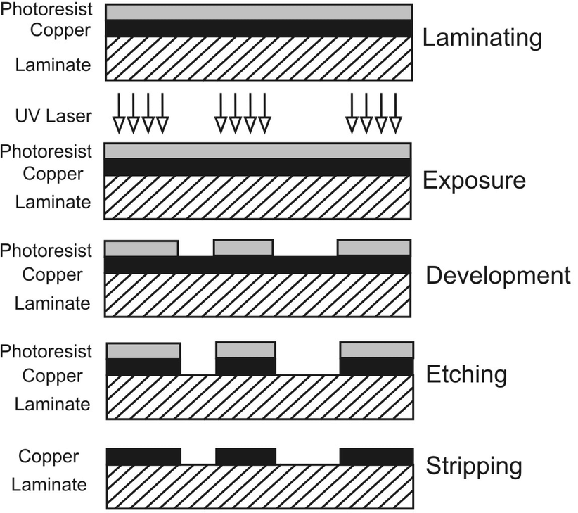
The Role of PCB Imaging in FabricationPCB imaging is a critical step in the fabrication process, where the circuit design is transferred onto the board. This process ensures that the copper traces, pads, and other features are accurately placed according to the design specifications. Let's explore what PCB imaging involves, the technologies used, and why it matters for the quality of the final product. What Is PCB Imaging?PCB imaging, often referred to as photolithography in traditional manufacturing, is the process of creating a pattern of the circuit design on the board's surface. It starts with a photosensitive layer, called photoresist, applied to the copper-clad board. The design is then projected or printed onto this layer using light or laser technology, hardening or softening specific areas of the photoresist. After exposure, the unneeded photoresist is washed away, leaving behind the pattern for etching, where unprotected copper is removed to form the circuit traces. This step is crucial because even a small error in imaging can lead to misaligned traces, short circuits, or open connections, rendering the board unusable. For high-speed designs, precise imaging ensures signal integrity by maintaining consistent trace widths and spacing, which directly affect impedance values (e.g., maintaining a 50-ohm impedance for RF applications). Technologies Used in PCB ImagingSeveral imaging technologies are used in PCB fabrication, each suited to different levels of precision and production needs:
The choice of imaging technology depends on the design requirements and budget. For instance, if you're designing a board with fine traces below 4 mils, investing in LDI might be necessary to ensure accuracy.
Impact of PCB Imaging on Cost and QualityPCB imaging not only affects the quality of the board but also influences the overall cost of fabrication. High-precision imaging methods like LDI, while more expensive, reduce the risk of defects and rework, which can save money in the long run, especially for complex designs. On the other hand, opting for cheaper imaging methods might lower upfront costs but could lead to higher failure rates during testing or in the field. For example, a misalignment in imaging could cause a trace to deviate by just 1 mil, potentially disrupting a high-speed signal traveling at 3 GHz, leading to signal loss or crosstalk. Investing in better imaging technology upfront ensures reliability, especially for critical applications in aerospace or medical devices.
How Board Components Influence PCB CostWhile material and imaging costs are significant, the components mounted on the PCB during assembly also play a role in the overall expense. The type, quantity, and availability of components can add up quickly, especially for complex designs. Component Selection and CostThe components used on a PCB, such as resistors, capacitors, integrated circuits (ICs), and connectors, vary widely in price based on their specifications and sourcing.
Designing with commonly available, standard components can help keep costs down. Additionally, using surface-mount technology (SMT) components instead of through-hole ones can reduce assembly costs due to faster automated placement, though SMT requires precise imaging and soldering processes. Assembly and Testing CostsOnce components are selected, the assembly process—soldering components onto the board—adds another layer of cost. Automated assembly for SMT components is generally cheaper per unit, often costing $0.01-0.05 per component placement, but manual assembly for prototypes or through-hole components can cost $0.50-1 per placement. Testing is another critical step that impacts cost. Functional testing to verify signal integrity (e.g., ensuring a 1 GHz signal propagates without loss) or in-circuit testing to check component values can add $1-5 per board, depending on the complexity. Skipping testing might save money upfront but risks costly failures later.
Balancing Cost and Quality in PCB FabricationFinding the right balance between cost and quality is essential in PCB fabrication. Here are some practical tips to optimize your project:
By understanding the interplay between PCB cost factors and the importance of imaging, you can make strategic decisions that ensure both affordability and reliability for your projects.
ConclusionNavigating the world of PCB fabrication involves a deep understanding of cost drivers like material selection, design complexity, and production volume, as well as critical processes like PCB imaging. From choosing cost-effective materials to investing in precise imaging technologies for accurate trace placement, every decision impacts the final cost and quality of your board. Whether you're designing a simple prototype or a complex multi-layer board for high-speed applications, keeping these factors in mind can help you achieve the best results within your budget. With the insights provided in this guide, you're better equipped to tackle your next PCB project with confidence and efficiency. Share · · · · The Role of Flux in PCB Wave Soldering: Selection, Application, and Residue RemovalMarch 16, 2026PCB wave soldering flux types include rosin, water-soluble, and no-clean options with varying activity levels for oxide removal and solder flow. This guide covers selection criteria, spray foam drop-jet application methods, residue removal processes, and alternatives like nitrogen blanketing to boost joint reliability and yields for engineers. Article Achieving Uniform Solder Fillets in PCB Wave Soldering: Process ControlMarch 16, 2026Achieve uniform solder fillets in PCB wave soldering with process control strategies. Optimize flux, preheat, wave height, conveyor speed for consistent fillet shape, height, and wetting balance. Includes visual inspection tips and troubleshooting for reliable through-hole assemblies. Boost quality in production. Article Optimizing Conveyor Speed for Efficient PCB Wave SolderingMarch 16, 2026Learn PCB wave soldering conveyor speed calculation to manage dwell time, immersion depth, and throughput effectively. Electric engineers get practical steps, best practices, and troubleshooting tips for higher process efficiency and fewer defects in wave soldering operations. Article Understanding IPC Standards for PCB Surface Finishes: Ensuring Quality and ComplianceMarch 11, 2026Understand IPC standards IPC 4552 ENIG and IPC 4553 immersion silver for PCB surface finishes. Ensure compliance, enhance solderability, and prevent common defects to achieve reliable, high quality circuit boards. Article High Speed Routing Techniques: PCBMarch 11, 2026Master high speed routing in PCBs to ensure signal integrity and minimize electromagnetic interference. Learn essential techniques for robust designs, from controlled impedance to differential pair strategies. Prevent performance issues and achieve reliable electronics. Article Miniaturization Challenges in PCB AssemblyMarch 11, 2026Navigate the complexities of high density interconnect PCB assembly and precise component placement. Learn to tackle miniaturization challenges, from tiny part handling to thermal stress, ensuring robust and reliable electronics. ArticleGet Instant PCB |